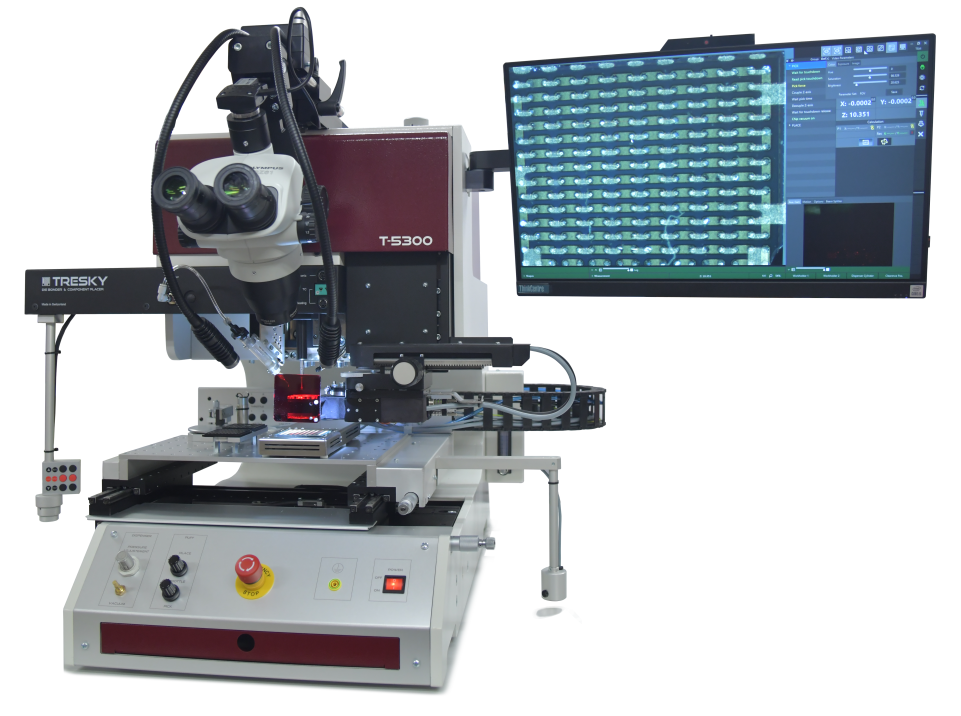
Search

T-5300-W

Semi-Automatic Die Bonder with wafer capabiltites

Tresky’s T-5300 is the flagship of our Die Bonders and adds a motorized, programmable Z-axis, with our True Vertical Technology™, to the repertoire of the universal T-5100, making it extra useful for repetitive processes in small-scale production, where operator influence must be minimized. The T-5300 really shines in applications with highest precision requirements, such as flip-chip, or eutectic placement. An optional high-resolution beam splitter unit allows sub-micron placement accuracy.

Like all Tresky Die Bonder this pick & place system operates with True Vertical Technology™.
The increased travel range on Z allows working on various bonding heights for Epoxy-, Eutectic- and Flip-Chip processes.

Quick Enquiry

If you want to know more about T-5300-W
Semi-Automatic Die Bonder with wafer capabiltites

T-5300-W

Manual Die Bonder with semi . process capabiltities
Wafer Handling capabiltities
Pick up from waffle, Gelpak or other.

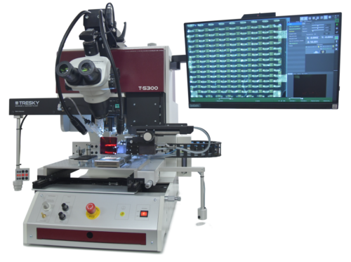
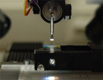
Tresky’s T-5300-W is the flagship of our Die Bonders and adds a motorized, programmable Z-axis, with our True Vertical Technology™, to the repertoire of the universal T-5100, making it extra useful for repetitive processes in small-scale production, where operator influence must be minimized. The T-5300 really shines in applications with highest precision requirements, such as flip-chip, or eutectic placement. An optional high-resolution beam splitter unit allows sub-micron placement accuracy.

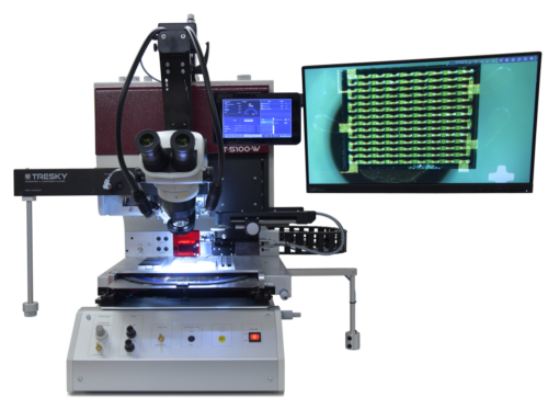
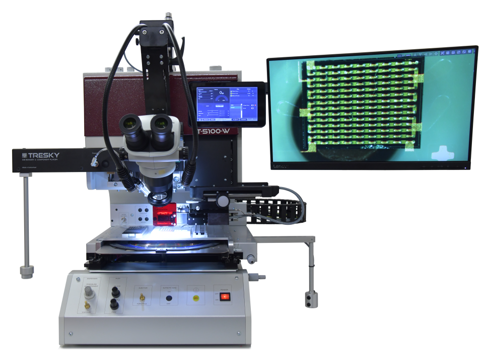
The systems can run all basic functions as well as the industries most advanced applications by adding a wide range of available options. As with all of Tresky’s products, the T-5100-W incorporates True Vertical Technology™ which guarantees parallelism between chip and substrate at any bond height. Together with superior ergonomics the platform is the industry’s most sophisticated system in its class and with the new intuitive software even easier to operate.

The extremely rigid machine, with its completely redeveloped base is compact and fits on a lab desk. It can be expanded with many different modules to cover an enormous range of applications.

Operating a Tresky die bonder/placer is intuitive. A few minutes’ training is sufficient to start working with the machine. The accuracy and repeatability of placing parts is superb thanks to a number of well thought out features like a true, linear Z-Axis, Force Control, XY Fine Control and high-resolution optics that allow flip-chip placing down to sub-micron accuracy.

Typical and customized applications :

  • Die sorting from wafer into waffle packs or gel packs
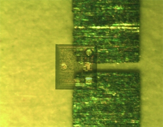
  • Die attach with adhesive (stamped or dispensed)
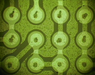
  • 3D packaging of MEMS, MOEMS, Photonics, …
  • High-precision placement with visual adjustment by beam-splitter unit for look-up inspection of edges, corners or patterns, e.g. for laser bars
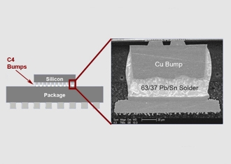
  • Flip-Chip with ultrasonic die attach
  • Flip-Chip with adhesives or anisotropic foils
  • Sensor assembly
  • UV curing of die attach
  • Eutectic bonding of AuSi, Copper Pillar and others
  • Ultrasonic bonding on a curved surface

XY- Movement (placement stage): 220mm x 220mm (manual)
Z- Movement: 120mm (automatic with Z-Measurement resolution ±0.001mm)
Spindle Rotation: 360° (unlimited)
Bond Force: 20g – 4000g
Max PC Boards-/Substrate Size : 400mm x 280mm
Placement accuracy: ±10µm; ±1µm (process and option depending)
Optical Resolution (Flip-Chip Optic 1x Option: 1.25µm
Optical Resolution (Flip-Chip Optic 2x Option: 0.625µm
Dimensions: 1155mm x 790mm x 728mm
Weight:  95kg (+30kg option depending)
Voltage:  110V / 220V

FLIP-CHIPRFIDCOPPER PILLAR BUMPSTHERMOSONIC FLIP-CHIP BONDING
FLIP-CHIP

Microelectronic assembly is the direct electrical connection of face-down (hence, “flipped”) electronic components onto substrates, circuit boards, or carriers, by means of conductive bumps on the chip bond pads. In contrast, wire bonding, the older technology which flip chip is replacing, uses face-up chips with a wire connection to each pad. Tresky’s modular die bonding equipment with the most common Flip-Chip option, based on a beam splitter vision system, allows high accuracy placement by one ore multiple points.

RFID

Most RFID (Radio-frequency identification) tags contain at least two parts. One is an integrated circuit for storing and processing information, modulating and demodulating a (RF) signal, and other specialized functions. The second is an antenna for receiving and transmitting the signal. Tresky’s modular die bonding equipment delivers, once more, optimal perfomance in R&D and pre-production assembly as e.g.: Bonding of a Flip-Chip to Antenna.

BONDING OF DEVICES WITH COPPER PILLAR BUMPS

Flip chip technology is keeping pace with the increasing connection density of the ICs and is capable of transferring semiconductor performance to the printed circuit board. The pitch is growing smaller, which means flip chip technology with solder bumps will unavoidably run up against its technical limitations. The reason for this is the spherical geometry of the bumps. The solution to this problem is copper pillars. In this contact technology for flip chip assembly, special cylindrical copper connections function with a solder deposit instead of the usual solder ball bumps to form the connecting element between semiconductor and substrate. The result: improved reliability and enhanced electrical and thermal connection characteristics, greater connection density with narrow pitching and RoHS conformity.

THERMOSONIC FLIP-CHIP BONDING

Thermosonic flip-chip bonding is an advanced, solderless technology for area-array connections. The approach is used to join ICs with gold bumps, Figure 1, to gold plated pads on substrate. It is a simple, clean, and dry assembly process using a bonding mechanism, Figure 2, similar to thermo-compression bonding, but with lower bonding pressure and temperature due to the introduction of ultrasonic energy. The thermosonic process was mainly used for wire bonding but has also great advantages for die attach applications. The pure thermocompression welding typically requires interfacial temperatures of the order of >300°C. This temperature can damage packaging materials, laminates and some sensitive chips. The thermosonic process is a combination of thermo- compression and ultrasonic welding that optimizes the best quality of each for the microelectronics usage. Typically, the interface temperature and the bonding force can be much lower; between 100 to 160°C and 20 to 50g/ bump, which avoids above mentioned problems.

Tresky T-5300-W Datasheet

Tresky Overview 2022