Search

X-Ray and Computed Tomography Inspection

Our X-ray (DR) and computer tomography (CT) system is designed to meet the requirements for safe, reliable, non-destructive testing of electronic, microelectronic, electromechanical and other small products.

It is also possible to inspect semiconductor components and electronic devices (solder joints) without having to disassemble the device.

  • X-Ray Inspection
  • Computed Tomography
  • Measurements of outer and inner structures

Quick Enquiry

If you want to know more about X-Ray and Computed Tomography Inspection

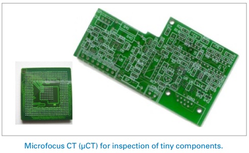
ELECTRONICS INSPECTION

Wafer and Surface-mount Device (SMD) Level Inspection

Typical inspection tasks include:

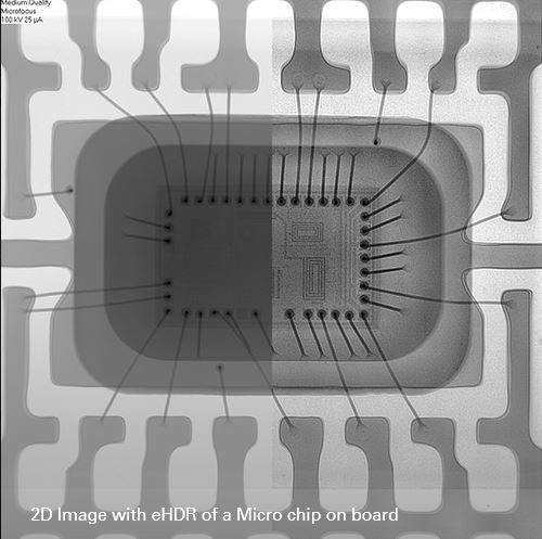
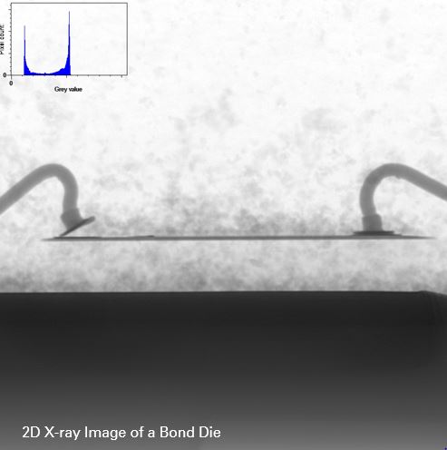
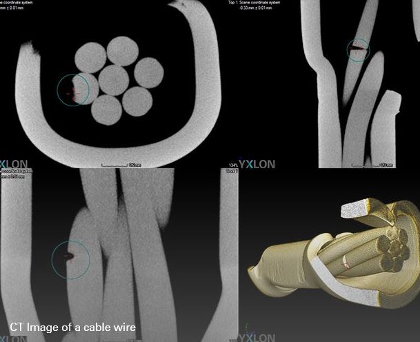
• Testing of bond wires and bonding areas
• Cavity analysis conductive and non-conductive chip bonding compounds
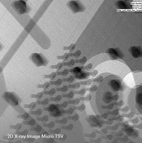
• Testing of 3D integrated circuits (IC) solder joints (micro bumps, copper pillars, Through-Silicon Vias (TSV))
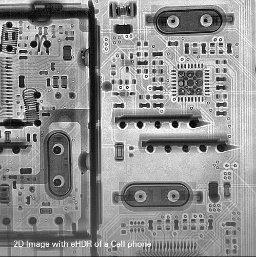
• Analysis of discrete components such as capacitors and coils

It is important to find cracks, open solder joints or voids via X-ray inspection. Additionally the measurement of pore sizes and their distribution is critical. Many of these inspections are performed automatically by the YXLON inspection systems for an improvement in the production process.
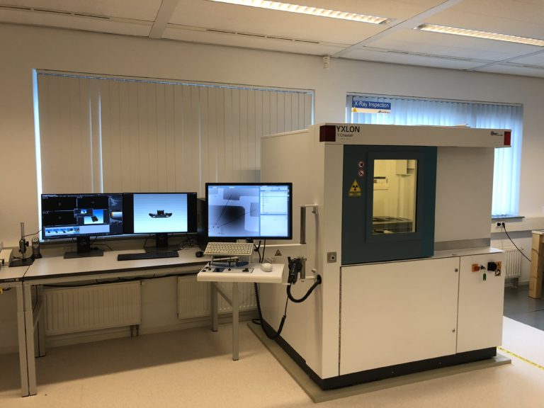
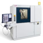
The YXLON CT systems provide the highest resolution 3D non-destructive failure analysis of semiconductor devices.

Multilayer Printed Circuit Board (PCB) Level Inspection

YXLON X-ray inspection technology is used in the production of multilayer printed circuit boards to measure the position offset and minimal residual ring width. High quality X-ray images in oblique view allow for the detailed observations.

• Visualization of individual layers
• Detection of defects
• Detection of failures

As an example, X-ray imaging can detect etching or layout errors, shorts caused by faulty interconnects and poor metallization of contact holes.

Assembled Printed Circuit Boards (PCBA) Level Inspection

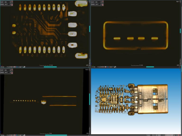
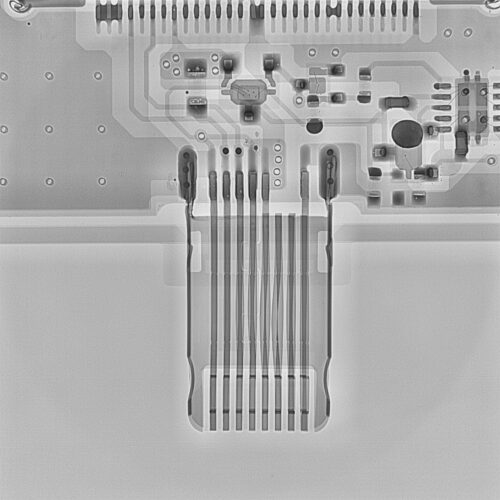
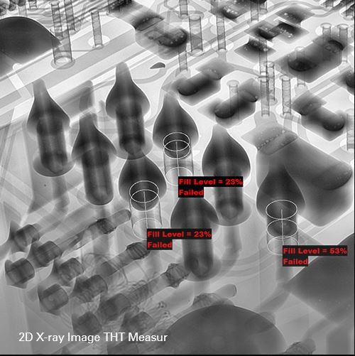
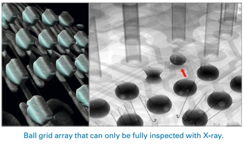
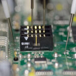
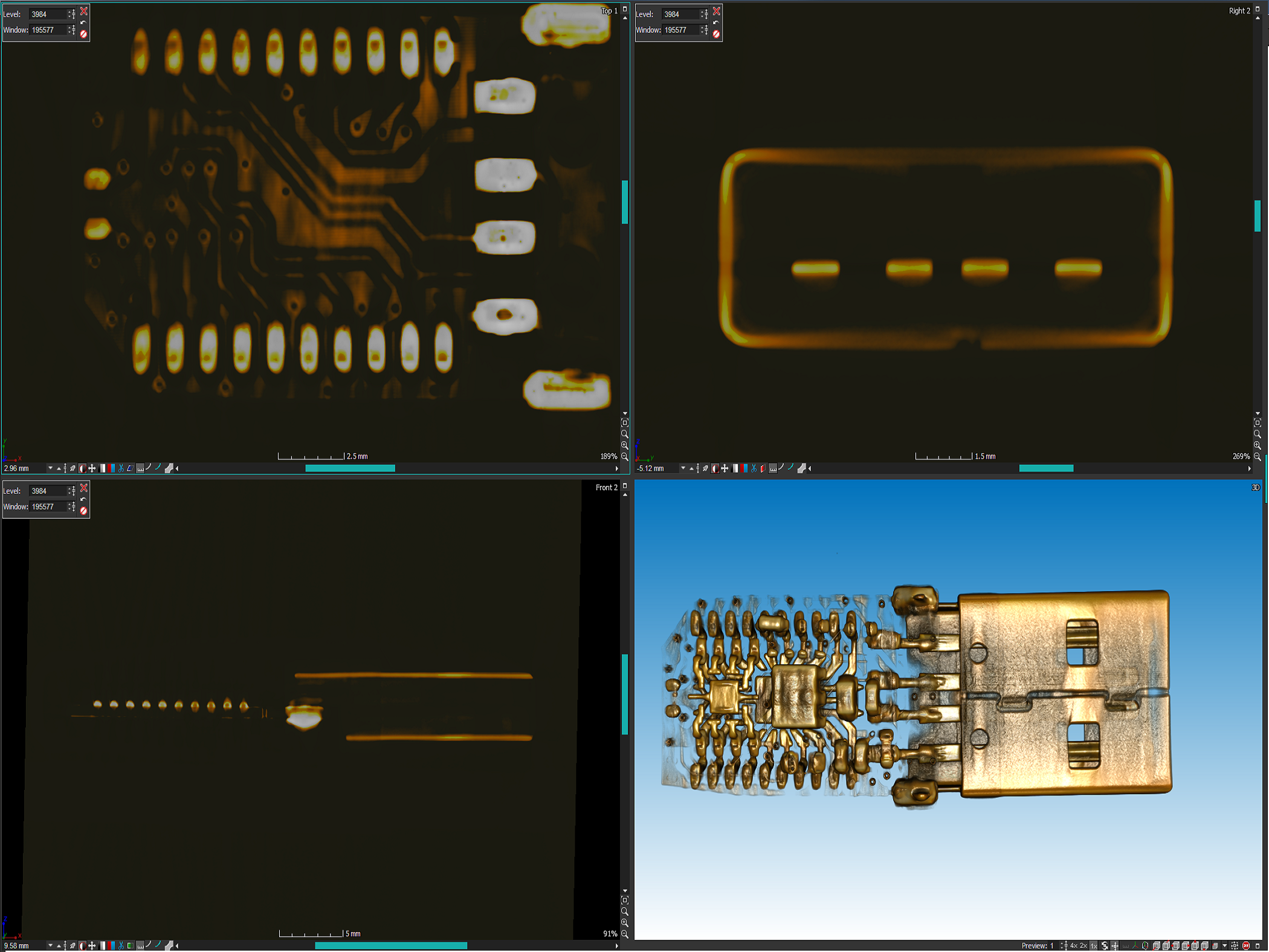
High-resolution YXLON X-ray imaging is widely used in failure analysis and production quality testing of electronic components, such as solder joint inspection. X-ray images help identify material defects and quality characteristics that influence the shape of the solder joint.

• Missing solder fillings
• Missing solder connections
• Solder voids
• Solder bridges
• Mistakes due to lack of wetting

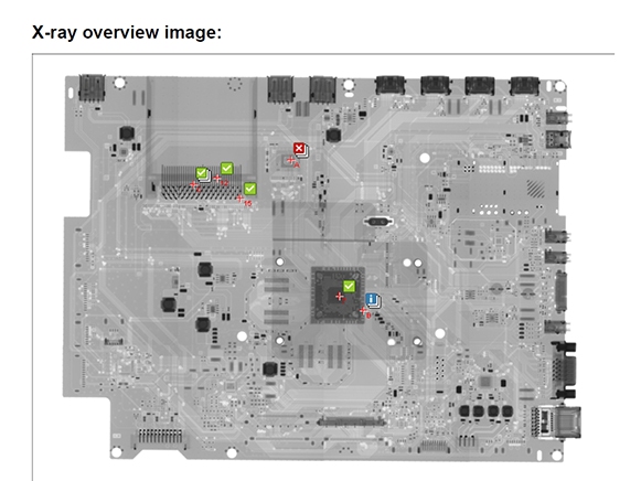
The semi-automatic testing software on YXLON X-ray systems allows for quick and easy ‘teach-in’ programming, as well as the highest fault coverage and repeatability.

Inspection of Specific Components

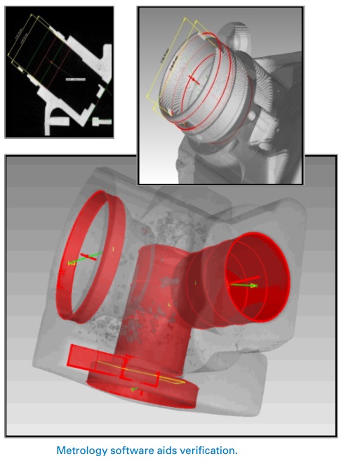
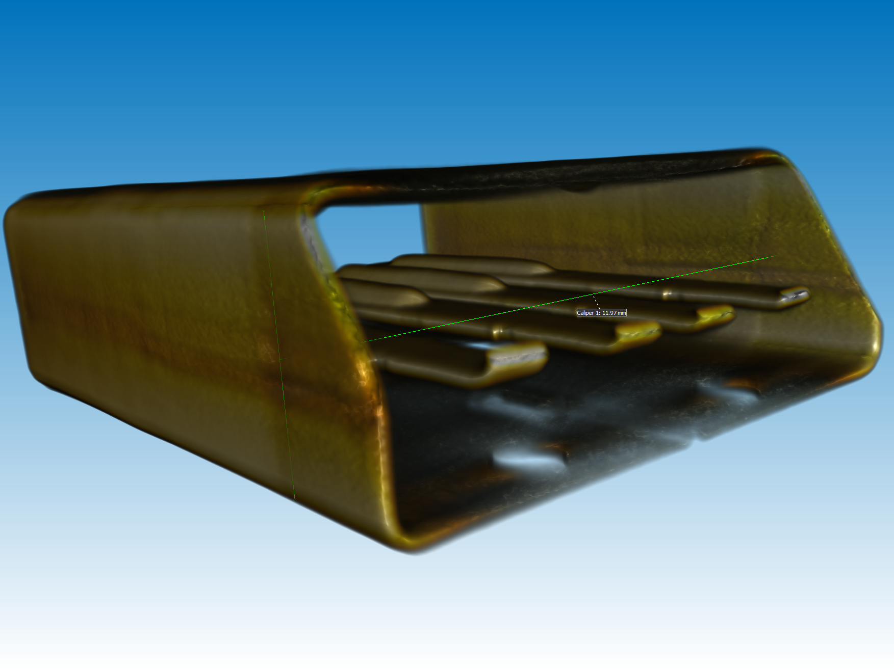
In components for power electronics (i.e. Insulated-Gate Bipolar Transistor (IGBT)) heat is passed over the solder joints to thick copper heat sinks. To achieve optimum heat transfer, the solder joints must be as free of voids as possible.
Although these hybrid components are often found within X-ray absorbing housings of tungsten and copper, which absorb X-rays to a high degree, high-contrast microfocus YXLON X-ray systems and detectors can be successful in solder joint inspection.
This is essential for the automatic calculation of absolute and percentage void size.

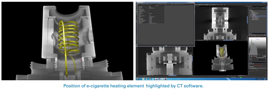
When testing sensors and electronic components, high-resolution YXLON X-ray techniques are used to inspect and to evaluate:

• Contacts
• Joints
• Packages
• Insulators
• Assembly


Electronic Components and PCB Assembly Analysis

This technique provides a deeper view into the tiniest components and assemblies within three-dimensional structures, offering detailed information about defects,such as the volume ofblowholes, the ball shoe size when a solder ball has lifted, or the pad surface structure of an unsoldered solder ball This in depth information simplifes root cause analysis.

The ball-grid array (BGA) shown in below figure is a form of component in which the solder joints are hidden between the component and circuit board As a result, X-ray technology offers the only way to perform a complete quality inspection of the solder joints.

Assembly Analysis

Computed Tomography (CT) is widely used to check the mechanical form and fit of assemblies.

CT is also often used to visualize components within a product, such as checking for the presence or orientation of components like gaskets or heating elements

Above figure shows the internal placement of a heating element for an e-cigarette

Our CT visualization software (VG Studio) allows operators to segment components and assign colors to the various items, such as the yellow used in above figure to highlight the heating element.

Measurements of Internal and Structures

Over the past few years, CT has become accepted as an alternative to a coordinate measurement tool.

It allows measurement of internal features without the need to destroy a part.  With good CT data scan, it is possible to verify many features quickly and with high accuracy.

Reverse Engineering & Inspection of 3D Printed parts

Multiple processes are available to assist with reverse engineering using CT

In one method , features can be measured based on their CT volume, then recreated using CAD software (e g , AutoCAD, SolidWorks, etc )

Another method is to extract regular geometry elements from a CT data set (cylinders, planes, etc ) and convert from an stl (standard tessellation language) file
to a STEP (Standard for the Exchange of Product Model Data).

For additive manufacturing (3D printing) applications, clean, high quality standard tessellation language (STL) fles can be input directly into a 3D printer Modeling software can be used to make minor changes.
In some cases, this application does not require reverse engineering software.

We can also inspect  3D printed parts on voids and other printing defects.

3D Movies of Electronics components for presentations

With our VG Studio Software we can make stunning high resolution 3D Video’s  of your components.
These video’s are widely used in websites, presentations and other  marketing material.


Accelonix X-Ray and Metrology Services Brochure