“It’s all in the mix – inline X-ray systems must be flexible and adapt to all required inspection tasks”, says Andreas Türk, Product Manager X-ray Inspection at GOEPEL electronic. What X-ray inspection tasks are possible with modern 3D AXI systems? In a free webinar GOEPEL electronics will answer these questions.
Tuesday November 3, 2020: 11:00 Central European time
The webinar will cover core system concepts available for inspection of SMD and THT solder joints using automated X-ray inspection.
The first part of the presentation will explain:
- Methods for 3D image acquisition: stop-and-go and scanning.
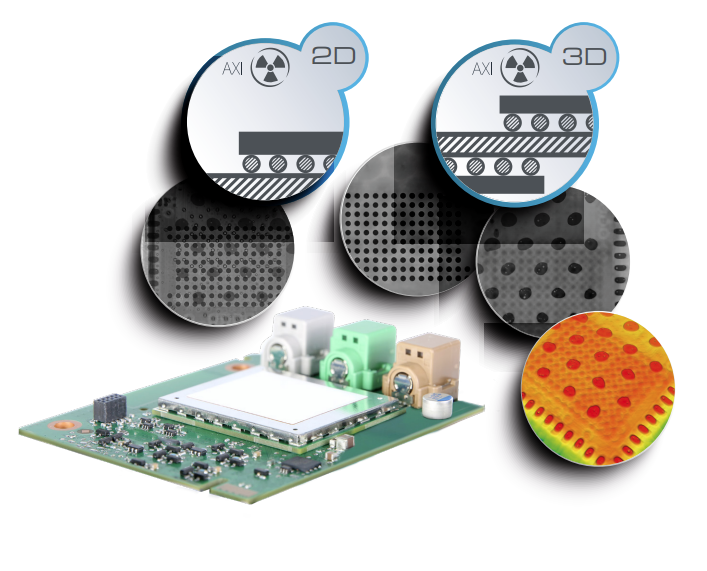
- Difference between 2D, 2.5D and 3D X-rays
- 100% solder joint inspection using GOEPEL 3D x-ray scanning technology within the PCB assembly production cycle .
- Practical examples how soldering defects can be reliably identified using fully automated 3D X-ray inspection.
- Range and limits of potential inspection tasks to outline 3D AXI process capability.
In the second part of the webinar, the topic of system software will be examined in more detail.
We will provide answers to the following common questions.
- How are inspection function parameters defined in 2D and 3D?
- How do you deal with warped circuit boards?
- What practical experience is there?
The webinar is aimed at quality and production managers directly involved with the manufacture of electronic assemblies.
It will also provide useful information for technologists, production planners and managing directors of companies using Electronics Manufacturing Service providers.