X-ray inspection is now a fundamental process in the manufacturing and quality assurance of printed circuit boards (PCBs). This non-invasive technique enables detailed observation of component interiors and solder joints, ensuring integrity without inflicting any harm. But how do 2D/3D inspections differ from computed tomography (CT) and laminography that utilizes 3D reconstruction, especially in the realms of microelectronics and PCB production? Let’s explore their mechanisms and the types of systems implemented.
X-ray Inspection Explained for PCBs
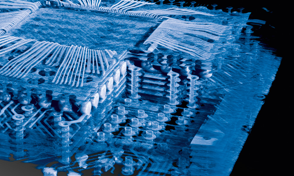
X-ray inspection is an important tool in the electronics manufacturing sector, particularly for inspecting printed circuit boards (PCBs). This non-destructive testing method uses the penetrating ability of X-rays to examine the internal structures and conditions of electronic assemblies thoroughly. By leveraging the differential absorption of X-rays based on material density and thickness, this technique provides a detailed view of internal components and connections that are usually hidden within complex PCB assemblies.
In the realm of PCB inspection, X-ray technology is especially useful for identifying hidden solder joints, securing components, and the intricate structural details of multi-layered circuit boards that are not visible through standard external inspection.
As X-rays penetrate the electronic board, variations in material properties such as density and thickness create different levels of absorption, which results in a projection image that captures detailed internal structures. This process reveals potential defects and anomalies that might not be visible on the surface but could lead to failures in the final product.
The most common issues detected during X-ray inspection of PCBs include short circuits, inconsistencies in solder quality, misalignment of components, and porosity within solder connections, all of which are important for ensuring the reliability and functionality of the PCB in its intended application.
Understanding 2D X-ray Inspection for PCBs
2D X-ray inspection is a method that utilizes X-rays to create two-dimensional images. This technique involves emitting X-rays from a source, which pass through the object being inspected and are captured by a detector on the opposite side. The degree to which these X-rays are absorbed varies based on the density and thickness of the material, resulting in a contrast image that is then processed to highlight details.
This method is valued for its speed, making it a common choice for inspecting printed circuit boards (PCBs). It is capable of detecting issues like short circuits, inconsistencies in solder, and component misalignments. However, 2D X-ray inspection does not provide depth information or the exact locations of defects, which may hinder the identification of some types of defects. Also, it cannot fully visualize the intricate internal structures of complex PCBs.
2D X-ray inspection is typically employed for examining solder joints and components on PCBs, as well as the inner layers of multi-layer PCBs. For PCBs with more complex and sophisticated internal structures, 3D inspection methods are often required to ensure thorough and accurate visualization. While multiple 2D scans from different angles can be combined to produce a form of 3D visualization, this approach lacks the precision and clarity provided by genuine 3D X-ray inspection techniques.
3D Computed Tomography (CT) Inspection with 3D Reconstruction for PCBs
3D computed tomography (CT) inspection is a sophisticated non-destructive imaging technique that utilizes X-rays to generate three-dimensional images of an object. This method stands apart from 2D inspection by providing comprehensive spatial information, enabling precise identification and localization of defects and anomalies within the object.
The core principle of CT inspection involves capturing numerous 2D images from various angles around the object. These images are then processed using a tomographic reconstruction algorithm, which compiles them into a detailed 3D image. This image can be manipulated to view the object from different perspectives, dissected for in-depth analysis, or utilized to assess the spatial characteristics of the object, such as dimensions and the exact nature of internal features.
The advantages of 3D CT inspection over traditional 2D methods are significant. It delivers exact spatial details, allowing for the accurate pinpointing of defects and abnormalities that might be concealed in 2D views, such as internal voids or foreign inclusions. This method also facilitates precise measurements of defect sizes and shapes.
Despite these benefits, CT inspection may sometimes fall short in resolution compared to 2D imaging. The resolution in a 3D image is dependent on the voxel size (3D pixels), which can be larger than the pixels used in 2D images, potentially affecting detail clarity.
3D CT inspection proves exceptionally valuable in the manufacturing and analysis of electronic boards, where it is used extensively for detecting defects, analyzing failures, and inspecting various components like solders, vias, and internal layers. It also measures critical spatial properties such as layer thickness and component heights. However, for certain PCB inspection applications, especially where high-resolution surface details are sufficient, high-quality 2D inspection might be adequate.
Laminography Inspection with 3D Reconstruction (CL)
Laminography serves as a powerful inspection method tailored for flat objects such as integrated circuits, electronic boards (PCBs), and various consumer electronics like phones, tablets, and laptops. It also applies to artifacts like papyrus manuscripts. This technology melds the benefits of 2D and 3D inspection techniques by integrating depth of field information into high-resolution 2D images, thus enhancing the capability to detect and localize defects.
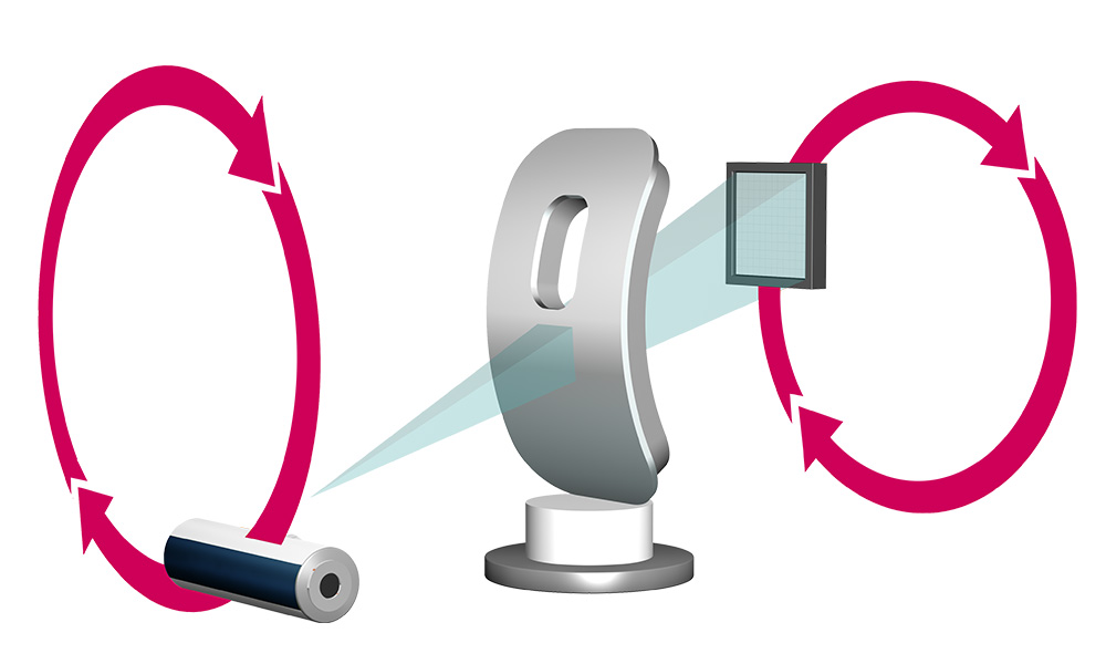
Differing from computed tomography (CT), laminography does not necessitate a full 360-degree capture to generate spatial data. It involves scanning the object from a limited angular range, enabling the X-ray tube to be positioned closer to the object, which results in higher resolution imaging.
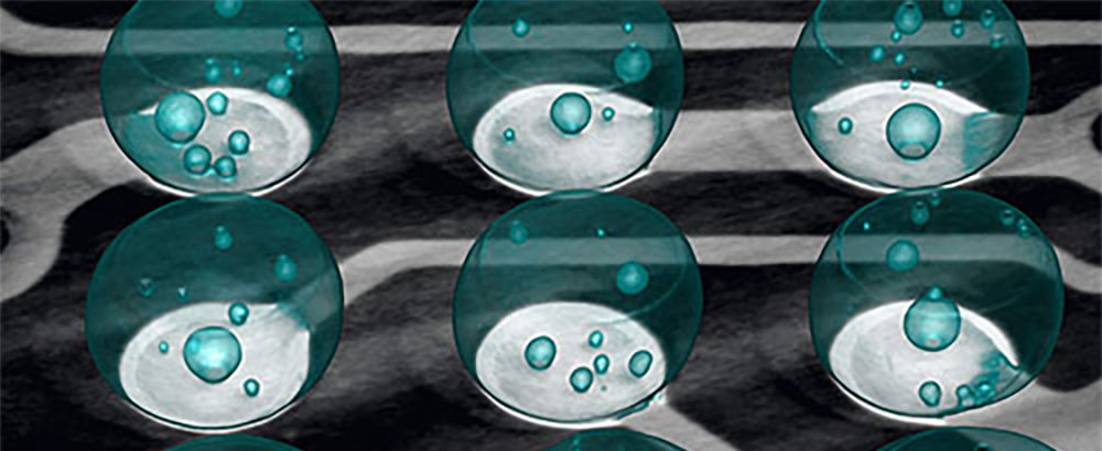
Laminography is prominently featured in various Comet Yxlon systems such as the Cougar EVO, Cheetah EVO, FF20 CT, FF35 CT, and FF85 CT. This approach is especially effective for inspecting solder connections on ball grid arrays (BGAs), verifying the adequacy of contact areas for electrical and thermal conduction and assessing the presence and distribution of voids.
For double-sided PCBs, the Comet Yxlon systems like the Cheetah EVO and Cougar EVO utilize laminography to produce clear layered images of contact areas, eliminating the visual obstructions caused by components on the opposite side that typically affect 2D radiographic images. The evaluation process of solders is supported by software such as the VoidInspect CL inspection workflow.
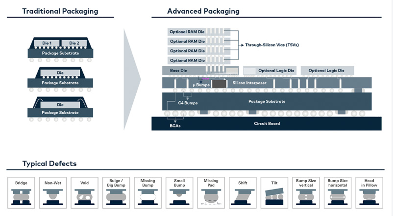
Moreover, laminography is adept at inspecting the connections between various layers in integrated circuits (ICs) and wafers. Given that IC packages comprise multiple layers, a simple 2D image often falls short, as it lacks spatial details and the internal structures tend to overlap. Systems like the Cheetah EVO and Cougar EVO leverage laminography to produce detailed images of the interconnection planes.
In the context of inspecting flat electronic devices such as tablets, mobile phones, and laptops, laminography excels as an inspection technique. During quality control and failure analysis phases, Comet Yxlon laminography systems ascertain the correct assembly and positioning of parts, or identify mechanical defects such as connection breaks.
In the rapidly advancing field of electric mobility, especially with the evolving configurations of battery systems in electric vehicles, ensuring safety and quality in mass production is imperative. For lithium-ion batteries, which are produced in large quantities, inspection processes must achieve high throughput without compromising resolution. Laminography, with its ability to deliver reliable and precise inspection of internal battery structures, reveals critical details like the geometry of stacked electrodes, the angles and overlaps of anodes, or the presence of foreign objects or voids, distinguishing it from traditional 2D testing methods.
Overview of Comet Yxlon Inspection Systems
Comet Yxlon provides a range of X-ray and CT inspection systems designed for specific tasks in semiconductor product evaluation.
2D Radioscopic Inspection: Ideal for quick, in-process inspections, the 2D radioscopic method excels in analyzing simple wire bonds, vias, and bumps. Systems like the Cheetah and Cougar offer rapid image generation with sub-micron resolution, ensuring high-quality imaging in minimal time. These systems are particularly suited for routine checks where speed and clarity are essential.
3D Tomography (CT): This technique is indispensable for conducting detailed 3D measurements that determine the spatial characteristics, exact locations, and dimensions of defects within components. It is primarily utilized for in-depth failure analysis. The CT technology is integrated into the FF20 CT and FF35 CT systems, which feature an intuitive user interface powered by Geminy software. Additionally, CT capabilities are optionally available for the Cheetah and Cougar systems, enhancing their versatility.
Laminography (CL): Laminography is critical for assessing the spatial properties of components and identifying the location and dimensions of defects, particularly in multi-layer packages and devices used in advanced packaging applications. The Cheetah and Cougar systems offer laminography with a vertical beam for the highest resolution, while the FF20 CT and FF35 CT systems provide a horizontal beam option, catering to different inspection needs and preferences. Each of these technologies is tailored to meet the demands of specific inspection requirements in the semiconductor industry, ensuring that manufacturers can maintain high standards of quality control and product reliability.