DfMExpress is a fully integrated DfM and DfA software enabling designers and electronic manufacturers to validate layout designs, prior to fabrication.
Design for Manufacturing – DfM
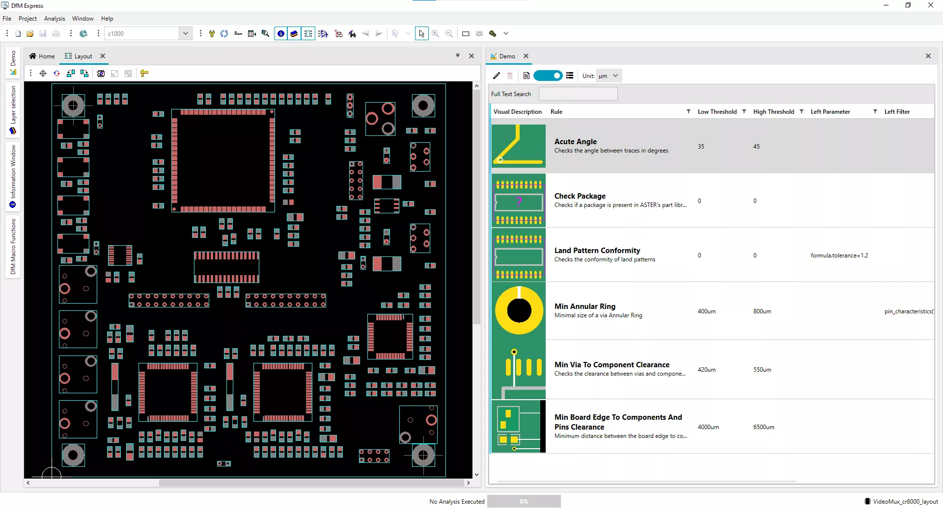
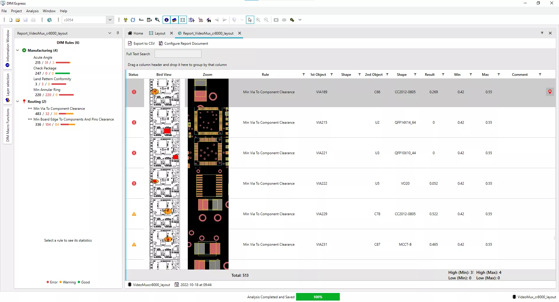
PCB fabrication is a complex operation, subject to a number of restrictions linked with copper, etching, drilling, solder mask…
- Small detail in copper might not be possible due to physical etching restrictions. A chosen technology e.g. IPC Class I should be applied everywhere on the board, as a single violation will force the PCB supplier to switch to more accurate parameters (e.g. IPC Class II) for the whole board. The finer the structures are, the more expensive the board fabrication will be.
- Copper and solder mask slivers: Narrow wedges of isolated copper or solder mask can sometimes float from their locations and reattach elsewhere on the board. If this happens with copper, it may end up shorting other nets together, while floating solder mask may expose copper that should normally be covered masked.ٚ
- As there will always be a slight displacement between the solder resist and the conductive pattern, the surrounding copper should have a clearance equal to the allowed displacement from the solder resist opening. If not, there is a risk that the surrounding copper will also be exposed, which can lead to short circuits.
- and many more rules need to be checked…
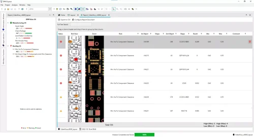
Design for Assembly – DfA
The automated assembly process will combine THT and SMD components to be placed and soldered on the bare board.
Here are a few examples of the kinds of errors that can be avoided by a Design for Assembly analysis:
- Insufficient clearance between parts, mechanical objects, and the board edge.
- Component placement errors: Components that are placed too close to each other, or at the wrong rotation or location in relation to each other, can cause problems during the soldering process.
- Incorrect land pattern pad sizes: Pads that are the wrong size, or not placed correctly for the part that will be soldered to it, can cause manufacturing problems. For small, two-pin passive components, this could cause unequal heating during soldering, resulting in the part pulling and standing up in a condition called “tombstoning.”
- ….
Mechanical design for Test – DfT
- Probes are placed by considering the mechanical and design for test (DfT) constraints practiced by respective companies.
- Probe locations may already be defined within the CAD data, but there may be insufficient access for total test coverage. In which case the probe analyzer can be used to consider alternative top and bottom side accessibility options such as through hole pins (THT), connectors, SMD pads, vias or bead probes etc.
- Once the possible probe positions have been analyzed, the nail allocation algorithm selects the best of these opportunities for the nail positioning according to the preferences set by the user.
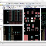
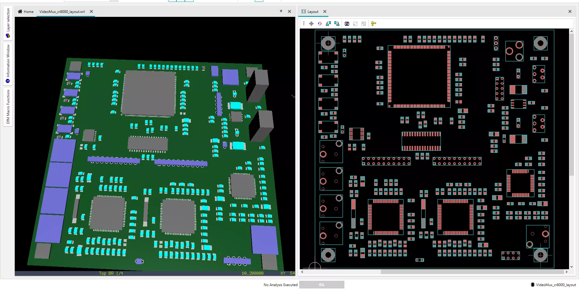
DfMExpress is powered by QuadView visualizer. Key features are:
- Create Layout views from standard formats such as ODB++, IPC-2581, FATF, GenCAD, or direct from native CAD layout data. No pre-processor needed.
- Import schematic from standard formats such a HPGL, PDF, EDIF etc.
- Search components, pins and nets throughout hierarchical designs and multiple sheets.
- Cross-probe between layout, schematic, and reports ٚ
- Capture snapshots of layout or schematic for cut & paste into your personal reports.
- Convert 2D layout view to 3D view and navigate through the board.


