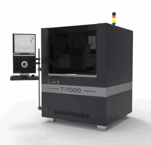


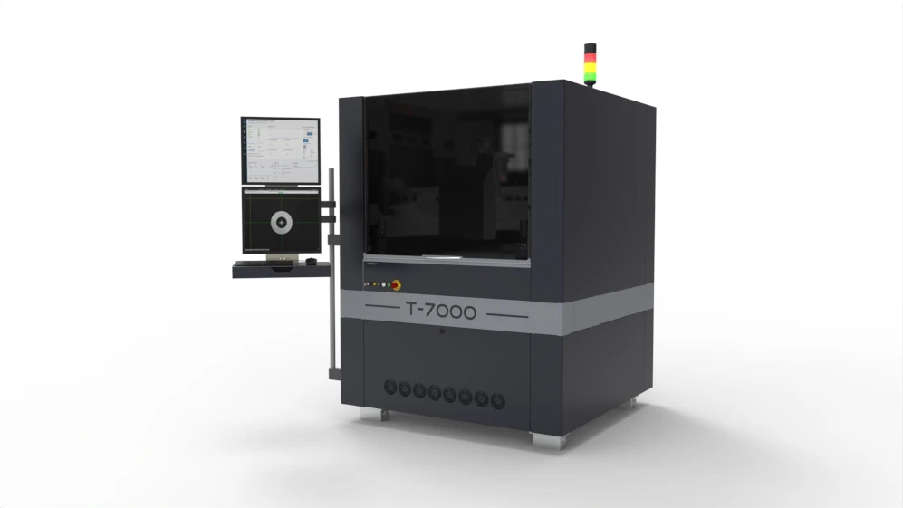
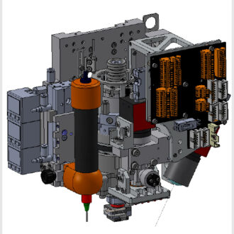
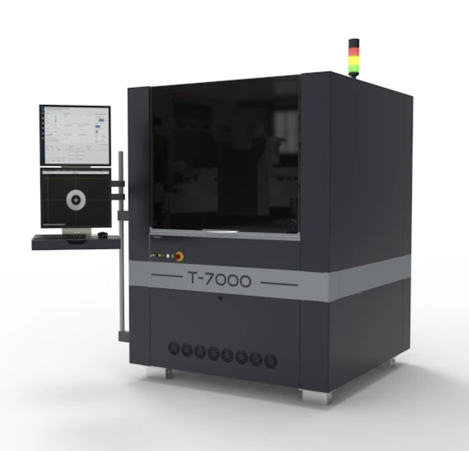
TRESKY T-7000 Photonics Bonder– High Precision Die Bonder for Nano & Opto Electronics
Leader in Micro-Assembly
Technological miniaturisation and functional integration in microelectronics and optoelectronics are essential for future-oriented product innovations. Micro-assembly and assembly and connection technology play a crucial role in the realization of these technological innovations in new and marketable products.
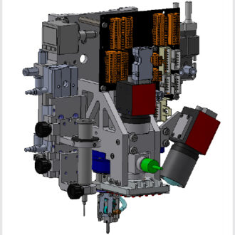
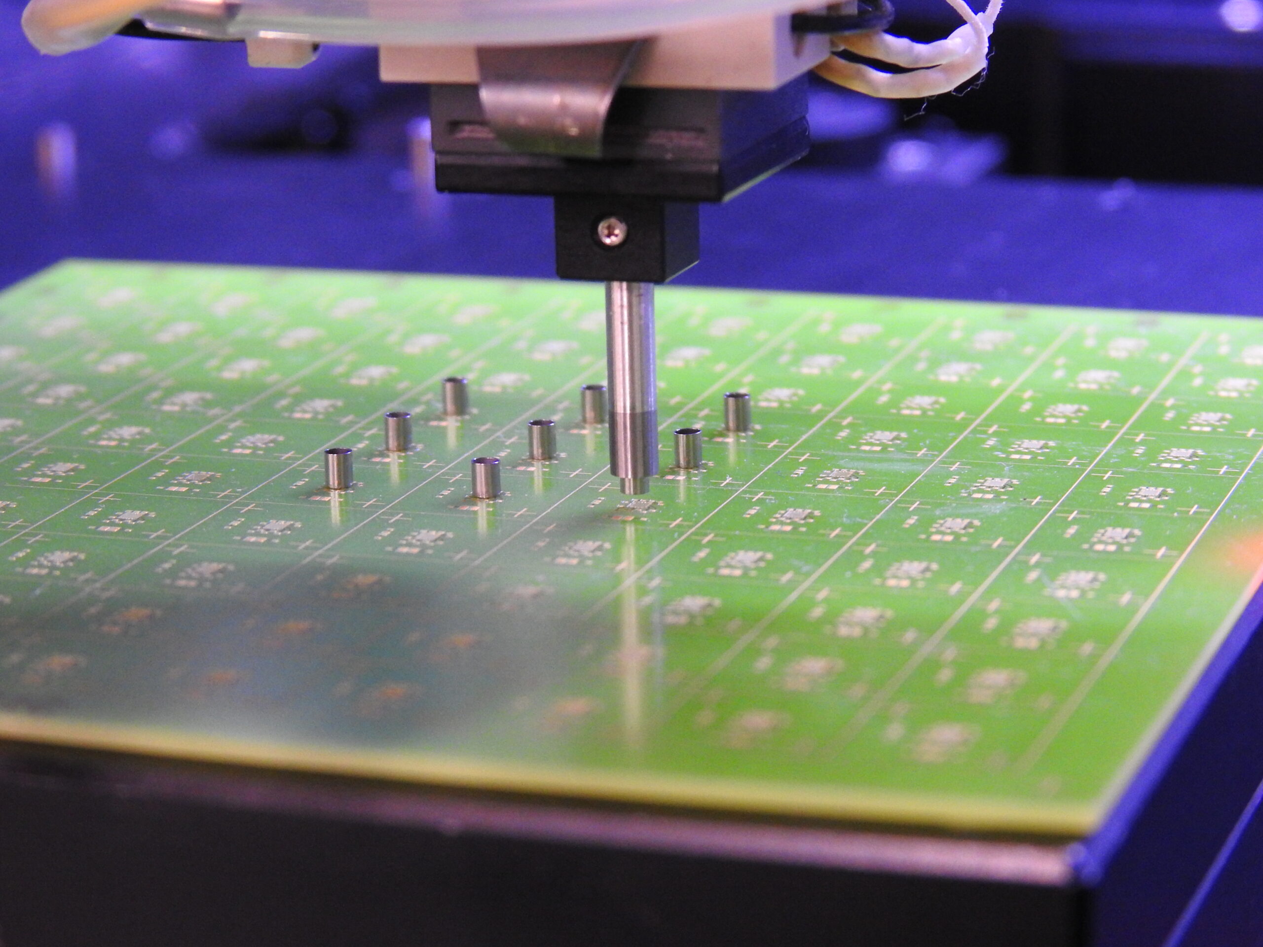
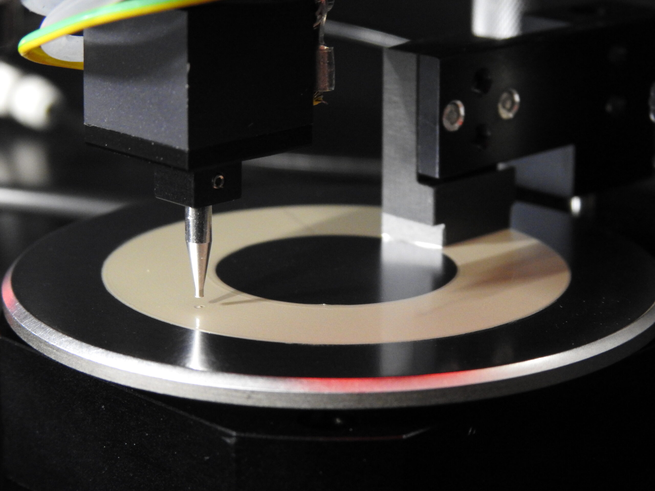
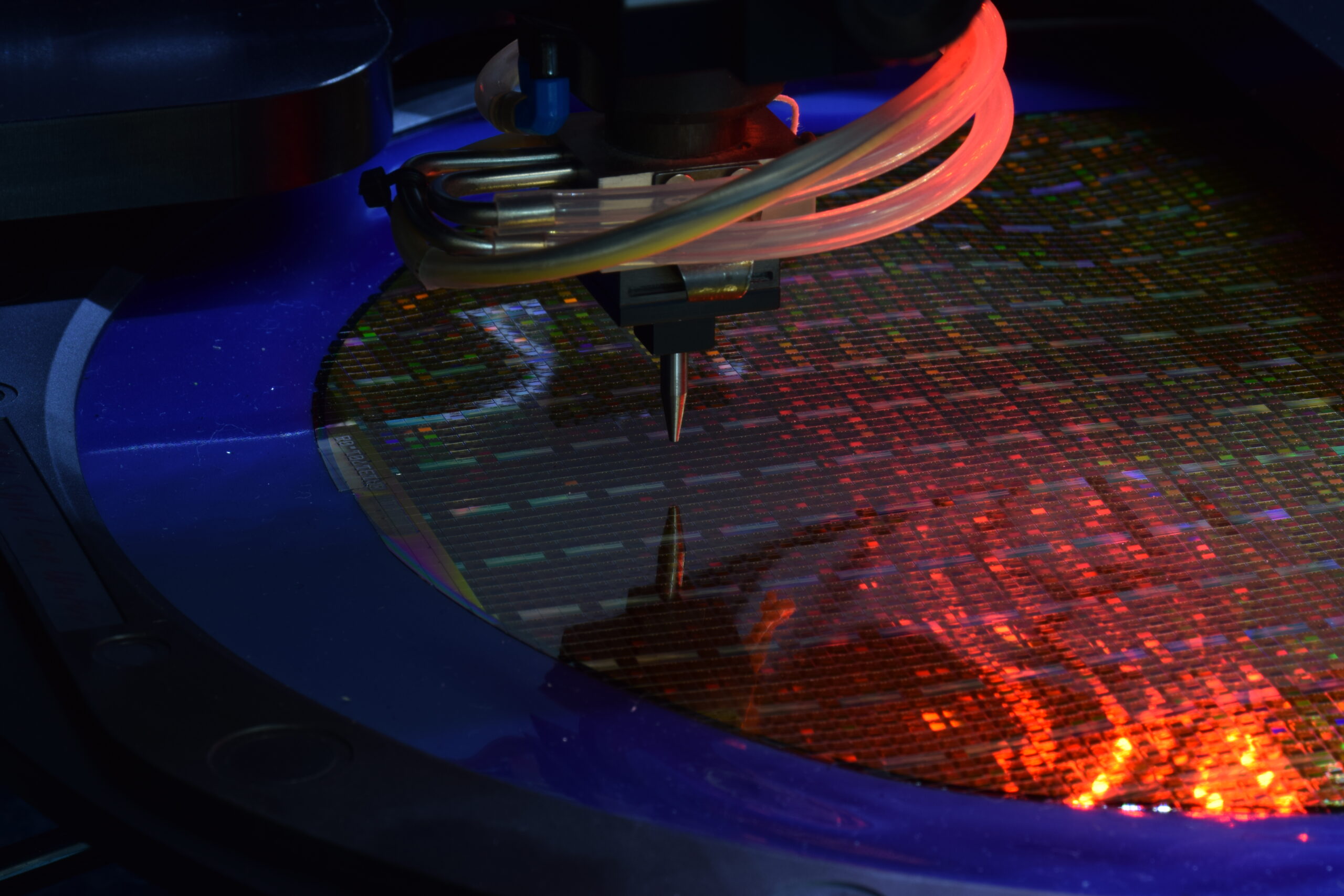
We have developed the T-7000 to successfully realize these requirements. The platform offers sub-micron placement accuracy, a travel range of 500 x 700 mm and a bonding head with minimum bonding forces of up to 0.01 N. On customer request, the bonding force range can be optionally increased to 100 N, 300 N or 500 N.
This model covers all common bonding technologies.
-
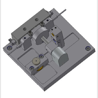
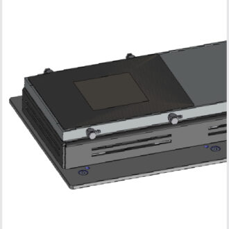
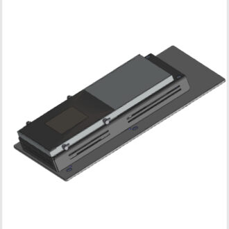
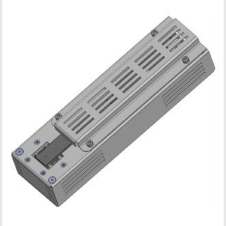
Modular design: Fully adaptable configuration for a wide range of applications.
-
High accuracy: < 1 µm placement precision at 3 Sigma.
-
Large working area: Ideal for multi-die and high-complexity assemblies.
-
Up to 300 N bonding force: Optional higher forces available.
-
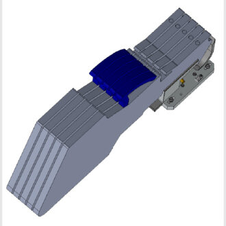
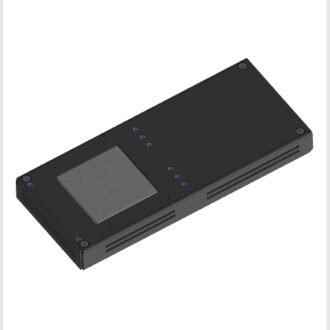
Flexible integration: Compatible with a wide variety of feeders, bond heads, and automation options.
-
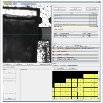
User-friendly software interface: Powerful GUI for programming, recipe management, and traceability.
-
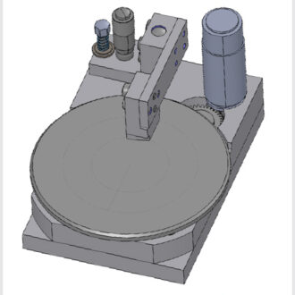
Bonding area: 500 x 700 mm with wafer table
-
Z-axis travel: 100 mm
-
Bond force range: 0.01 – 300 N (higher optional)
-
Placement accuracy: < 1 µm @ 3σ
-
Chip size range: < 0.05 mm up to large format
-
Axes resolution: 0.001 µm (XYZ), 0.005° (theta)
-
Tool rotation: 360°
-
Max acceleration: 2.5 G
-
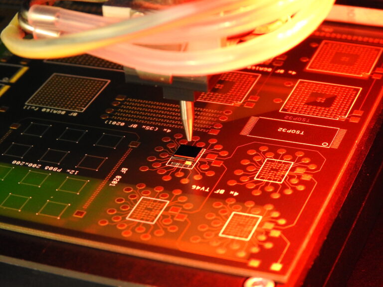
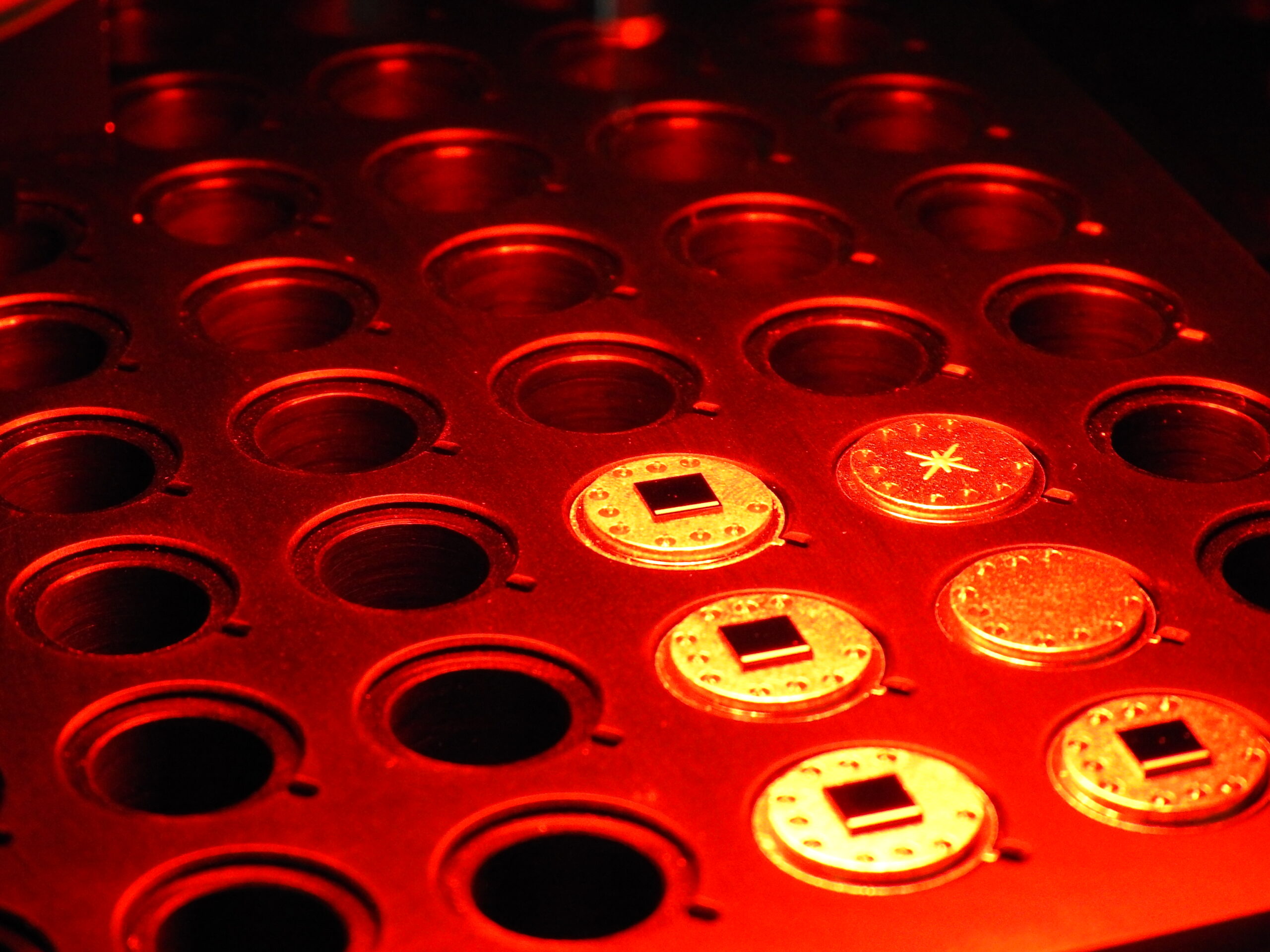
Photonics packaging
-
MEMS devices
-
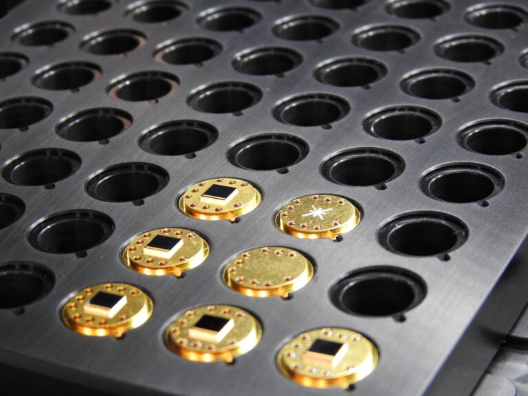
VCSEL & TO Header assembly
-
RFID and smart labels
-
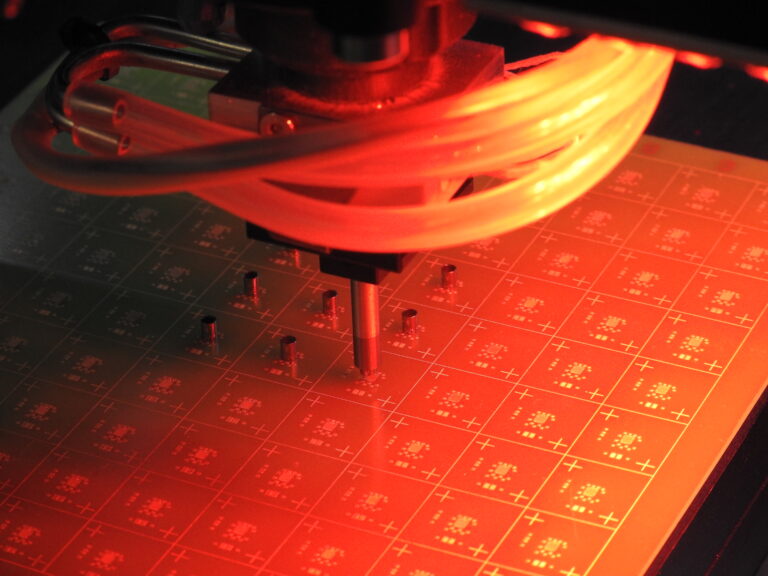
3D integration and SiP modules
-
R&D and pilot production
-
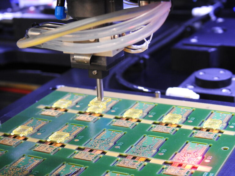
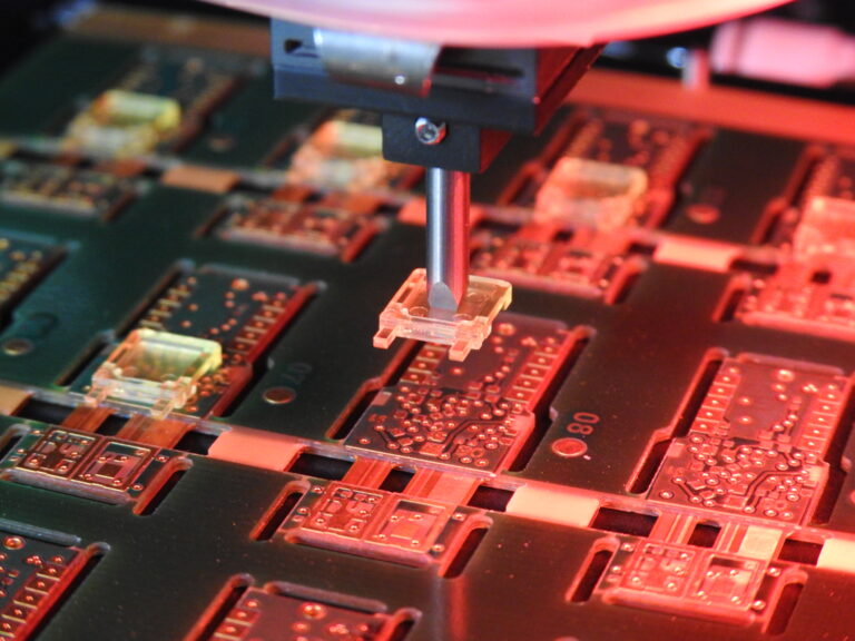
Flip-chip bonding
-
Epoxy & eutectic bonding
-
UV bonding
-
Thermocompression bonding
-
Photonics & glass bonding
-
MEMS & SiP assembly
-
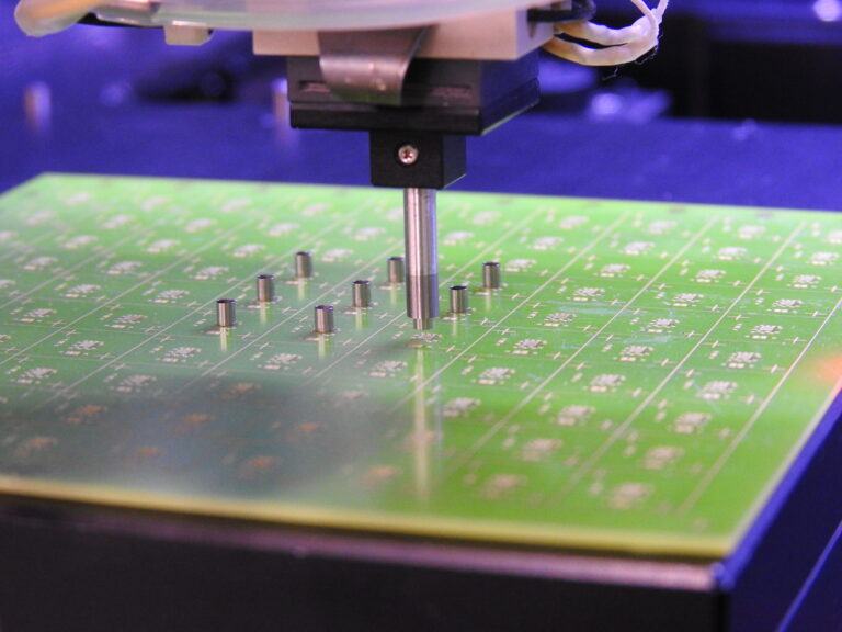
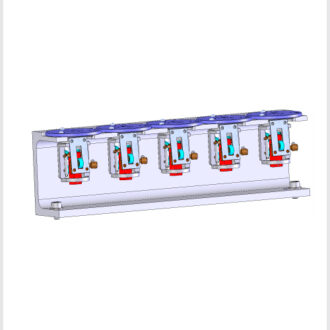
Die sorting and multi-die placement
-
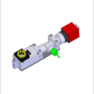
Advanced vision systems with WRGB ring light
-
Heated tools & bonding stages (up to 450°C)
-
Scrubbing and stamping units
-
UV curing units
-
Automatic tool changers
-
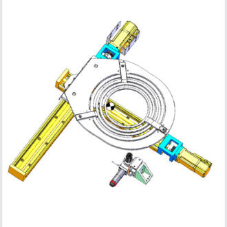
Wafer handling & ejector stages
-
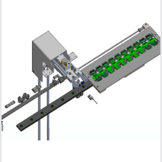
Component feeders (waffle pack, tape, tray, etc.)
-
ID scanning & traceability systems
-
MES integration & wafer mapping
-
Nitrogen or formic acid atmosphere for sensitive processes

