Inline AXI Inspection
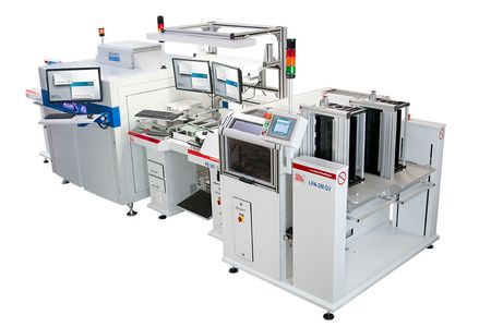
Inline AXI X-Ray systems for high-end inspection in mass production of printed circuit boards
The main task of an AXI X-ray system is the automatic detection of solder defects in both hidden and visible solder joints.
Inline AXI systems enable fully automatic loading, inspection, evaluation and result logging of PCB assemblies.
Depending on the requirements, two basic inspection strategies are usually used. On the one hand, there is a need for full-surface X-ray inspection of all components and solder joints, both hidden and visible solder joints, for example on SMD components such as SO-ICs.
In other cases, only selected, hidden solder joints need to be inspected with X-ray, as an AOI system, for example, inspects the remaining solder joints.
Modern AXI X-ray systems have a variety of inspection functions to detect soldering defects. Similar to an AOI system, an inspection program is created and parameterised on the basis of CAD data.
As an example, a BGA inspection includes checking of misalignments, solder bridges, solder joint diameters, head-in-pillow connections and voids.
The same applies to components such as QFN (Quad Flat No Leads Package) DFN (Dual Flat No Lead), QFP (Quad Flat Package) and LGA (Land Grid Array).
For THT solder joints, the tin penetration can be checked by X-ray inspection, and the rear solder miniscus can be assessed on gullwing pins that are difficult to see.
In large solder joints such as DPAK/TO-252 packages, but also in BGA solder joints, the detection of air inclusions (voids) is a specific X-Ray task.
Accelonix Services
Our Partners


