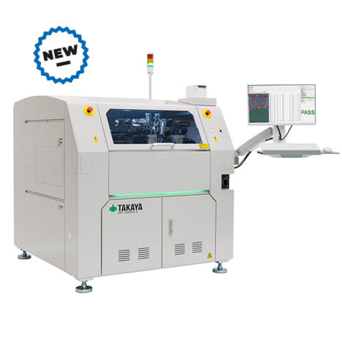
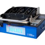
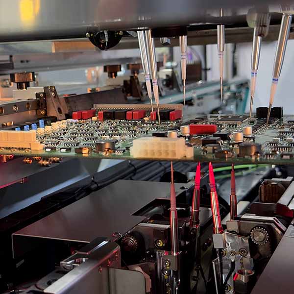
APT-2600F

Dual-Sided Flying Probe Tester New Generation 2025

The APT-2400F series is a high-performance flying probe test system with 4 heads and 6 flying probes.
It accurately contacts the extremely small pads on miniaturized PCBs, conducting tests in a short time.
With an advanced measurement system and a wide range of testing functions, it significantly improves test coverage and helps detect assembly defects and perform failure analysis that were previously difficult to identify.

For inline testing application, Accelonix can provide a turn key solution including magazine loading and unloading, pass/fail sorter, flip station and more handling solutions.

Quick Enquiry

If you want to know more about APT-2600F
Dual-Sided Flying Probe Tester New Generation 2025

The APT-2600F series is a high-performance flying probe test system featuring 4 heads with 6 probes on the top and 2 heads with 4 probes on the bottom, allowing simultaneous dual-sided testing.
This setup improves test coverage, reduces test time, and eliminates the need for board flipping, lowering the risk of damage.

With models supporting large PCB sizes and automation, it provides a cost-effective solution for prototype to mass production, enhancing PCB assembly quality.

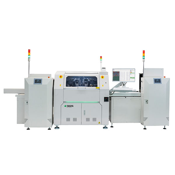
All models are available as inline machines. By connecting with a loader/unloader (available at Accelonix), you can build a continuous automatic test line with a maximum speed of 40 m/min. This allows for a smooth production line and efficient board inspection.
It provides an optimal in-line inspection environment for your manufacturing process, helping to achieve both productivity and quality control.

  • Dual-Sided Probing: Simultaneous top and bottom testing with up to 6 probes, improving test coverage and efficiency.
  • Sophisticated Measurement System: Uses a 16-bit DC source and AC generator, providing in-circuit and functional testing with optimal measurement accuracy.
  • Impact-Minimizing Probe Control: Slows probe speed to zero before contact, reducing stress on contact points and preserving board integrity.
  • High-Resolution Vision System: Equipped with a camera and liquid lens technology, offering clear imaging across varying component heights for OCR and AOI.
  • Distance Sensor: Measures PCB and component heights to detect lifted parts and ensure accurate contact.
  • 3D Imaging Capability: Generates 3D real maps for checking top-to-bottom net connections and areas that are difficult to inspect.
  • Temperature Sensor: Measures V-I curves and performs non-contact measurements for enhanced detection of component failures.
  • LED Color Sensor: Detects LED color variations by measuring hue, saturation, and brightness, ensuring precise inspection without extra fixtures.
  • Industry 4.0 Compatibility: Integrates with factory networks, enabling quick traceability, inspection visualization, and efficient issue resolution.
  • IC-OPEN Solder Failure Detection: Detects solder issues on IC leads within bus circuits, addressing a common challenge with QFP and BGA inspections.
  • Multi-Probe System: Supports simultaneous bottom-side contacts, integrating with external devices like ISP.
  • Automatic Probe Cleaning: Built-in cleaner removes contaminants from probe tips at preset intervals, ensuring stable and accurate testing results.
  • Industry 4.0 Ready: Integrates with factory networks for traceability and fast issue response.
  • 16 Bit DAC/ADC measuring unit incl. 3 x DC 4-Quadrant sources and measurement system
  • R, L, C measurements
  • Measuring voltage < 0,1V
  • Kelvin measurements
  • Guard functions
  • Diodes & Zener diodes measurement functions
  • Voltage Controller/Operational Amplifier
  • Transistors/FET/Optocoupler/Relays/etc.
  • DC/AC Current- and Voltage Measurements
  • Dynamic curve measurements of components and circuits
  • Isolation Tests
  • Continuity test
  • Frequency measurements
  • AC signal generator
  • Cluster tests
  • IC Open sensor
  • LED Sensor (wave length and brightness)
  • Temperature Sensor
  • Integration of external power supplies and test equipment(Boundary Scan, In System Programming, etc.)
  • Model Options: Available in standard and large sizes to accommodate different PCB dimensions.
  • Testable PCB Sizes: Supports a maximum PCB size of up to 985 mm x 610 mm.
  • Probes Configuration: Top probes include 4 tilted and 2 vertical probes, while the bottom features 2 fixed probes and 2 vertical probes.
  • Component Height: Maximum component height of 60 mm on the top and 120 mm on the bottom.
  • Component-Free Area: Minimum required area of 3 mm on both sides (7 mm optional for large configurations).
  • Test Speed: Single test at 0.05-0.06 seconds per step; combination test at 0.02-0.03 seconds per step.
  • Positioning Precision: Flying probe positioning repeatability within ±25 µm.
  • Minimum Pad Size: Capable of testing on pads as small as 50 µm.

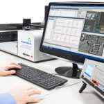
Goepel Takaya Boundary Scan Integration  

TestWay Express is a fully integrated solution that enables electronic manufacturers to optimize the design to delivery flow by:

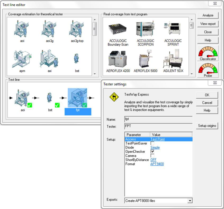
  • Defining the manufacturing line; including a combination of assembly, inspection and test machines.
  • Placing test probes intelligently to maximize the coverage and minimize the fixture costs, both initially and in the event of required modifications.
  • Estimating the test coverage for each individual strategy using theoretical models and optimize the combined results.
  • Generating input files for each test stage that reflects the test options for the selected strategy.
  • Measuring the real test coverage by importing the post-debug test program or coverage data.
  • Comparing the early estimation with the actual measured test program coverage, identifying gaps in the overall strategy.

The capability to generate lean test programs has particular benefits for the Takaya flying probe tester by:

  • Reducing debug time: Machine capability models, automatic test creation algorithms, optimum probe angle selection methods and advanced circuit analysis work together to reduce the amount of machine debug time required after output, thereby increasing machine capacity.
  • Increasing Test coverage: Push through technology allows automatic simple cluster testing to increase test coverage through low value resistive components.
  • Reducing engineering effort: Automatic component modelisation and intelligent opportunity assessment work together to save engineering time.
  • Increasing machine speed: Advanced circuit analysis algorithms allow the creation of tests to target the failure opportunities with no superfluous tests.
  • Reducing machine workload: Powerful test coverage analyzers work within the machine capability models to allow the optimization of combined tests across multiple machines, in order to achieve a lean test strategy.

Click here for more information.

APT-2600F Brochure: please contact us!

Contact

Newsletter

Subscribe to our Accelonix newletter and be informed about our newest products and our workshops.