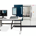
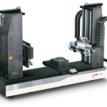
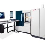
High Resolution CT Systems
Non-Destructive X-ray Inspection Technology for Electronics
YXLON industrial X-ray (DR) and computed tomography (CT) inspection systems are designed to meet requirements for safe, reliable, non-destructive testing of electronic, microelectronic, and electromechanical products.
Electronic components are becoming increasingly miniaturized. High-resolution and high-magnification YXLON industrial X-ray and computed tomography (CT) inspection systems provide the necessary tools for the examination of such components.
Typical surface-mounted device (SMD) inspection tasks include:
- Testing of bond wires and bonding areas
- Cavity analysis conductive and non-conductive chip bonding compounds
- Testing of 3D integrated circuits (IC) solder joints (micro bumps, copper pillars, Through-Silicon Vias (TSV)) in processor packages
- Analysis of discrete components such as capacitors and coils
It is important to find cracks, open solder joints or voids via X-ray inspection. Additionally the measurement of pore sizes and their distribution is critical. Many of these inspections are performed automatically for an improvement in the production process.
Our YXLON industrial CT inspection systems provide the highest resolution 3D non-destructive failure analysis of semiconductor devices.
Accelonix Services
Our Partners
